

ELECTRONIC PRINCIPLES - OD1647 - LESSON 1/TASK 2
different techniques will be discussed briefly in the following
paragraphs.
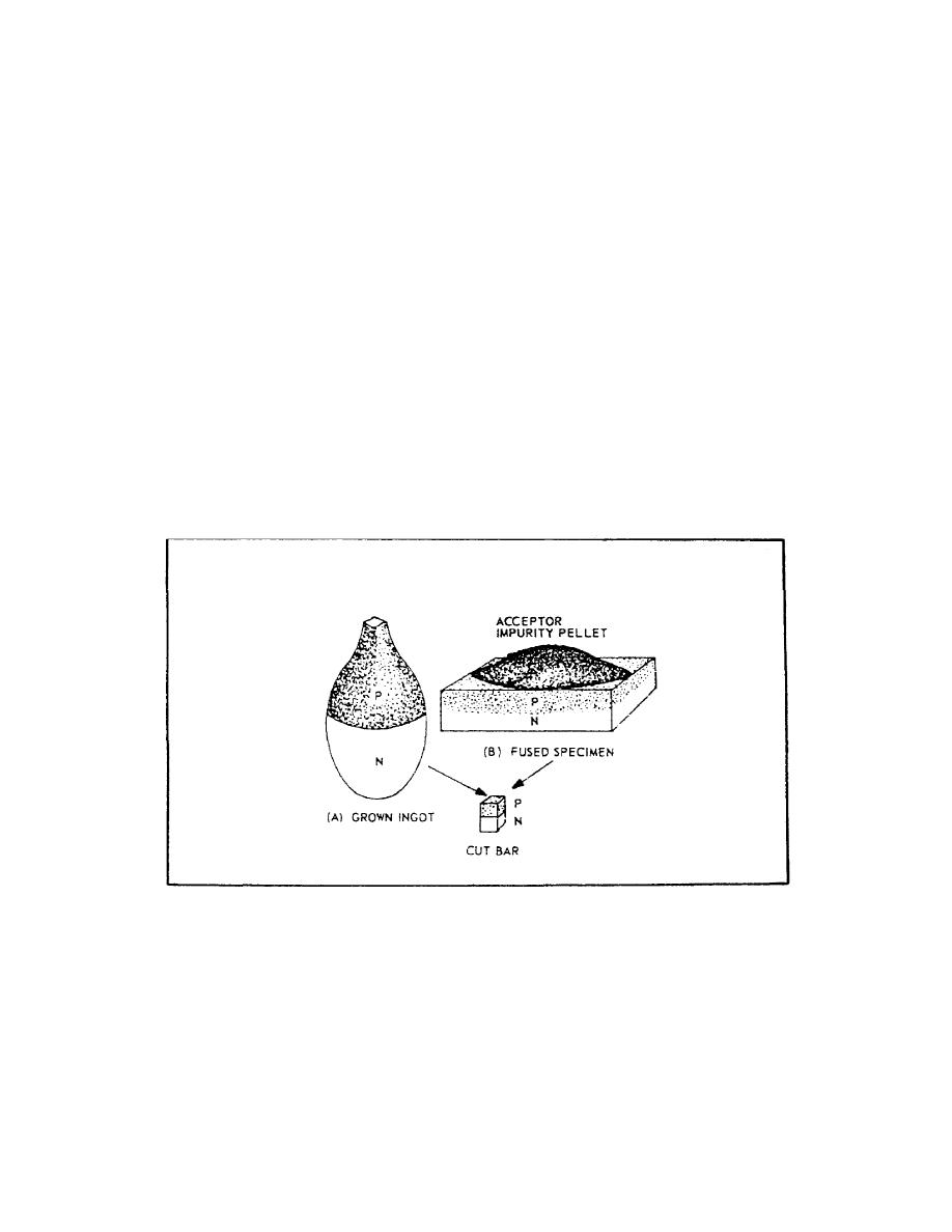
(1) Grown. In this method of manufacture, Ptype and Ntype
impurities are mixed into a single crystal. By so doing, a P
region is grown over part of a semiconductor's length and an N
region is grown over the other part. This is called a GROWN
junction and is illustrated in figure 77, view A.
(2) Alloy or FusedAlloy. In this method, an impurity of one
type is melted into a semiconductor of another type impurity.
For example, a pellet of acceptor impurity is placed on a wafer
of Ntype germanium and heated. Under controlled temperature
conditions, the acceptor impurity fuses into the wafer to form a
Pregion within it, as shown in view B of figure 77. This type
of junction is known as an ALLOY or FUSEDALLOW junction and is
one of the most commonly used junctions.
FIGURE 77. GROWN AND FUSED PN JUNCTIONS.
(3) PointContact. Figure 78 on the following page shown a
POINTCONTACT type of construction. It consists of a fine metal
wire, called a cat whisker, that makes contact with a small
amount of a Ntype semiconductor as shown in view A of figure
78. The PN union is formed in this process by momentarily
applying a highsurge current to the wire and the Ntype
semiconductor. The heat
112


 Previous Page
