

ELECTRONIC PRINCIPLES - OD1647 - LESSON 1/TASK 2
f. NType Semiconductor. An Ntype semiconductor is one which
is doped with an Ntype or donor impurity (an impurity that
easily loses its extra electron to the semiconductor, causing it
to have an excess number of free electrons). Since this type of
semiconductor has a surplus of electrons, the electrons are
considered the majority current carriers while the holes are the
minority current carriers.
g. PType Semiconductor. A Ptype semiconductor is one which
is doped with a Ptype or acceptor impurity (an impurity that
reduces the number of free electrons causing more holes). The
holes in this type semiconductor are the majority current
carriers since they are present in the greatest quantity while
the electrons are the minority current carriers.
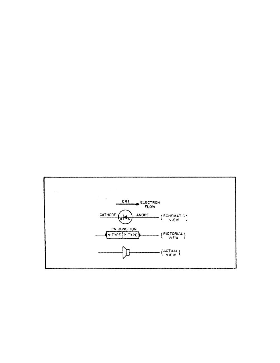
h. Semiconductor Diode. The semiconductor diode, also known as
a PN JUNCTION DIODE, is a twoelement semiconductor device that
makes use of the rectifying properties of a PN junction to
convert alternating current into direct current by permitting
current flow in only one direction (figure 76).
FIGURE 76. THE PN JUNCTION DIODE.
i. PN Junction Construction. A PN junction construction varies
from one manufacturer to the next. Some of the more commonly
used manufacturing techniques are: GROWN, ALLOY or FUSEDALLOY,
DIFFUSED, and POINTCONTACT. Each of these
111


 Previous Page
