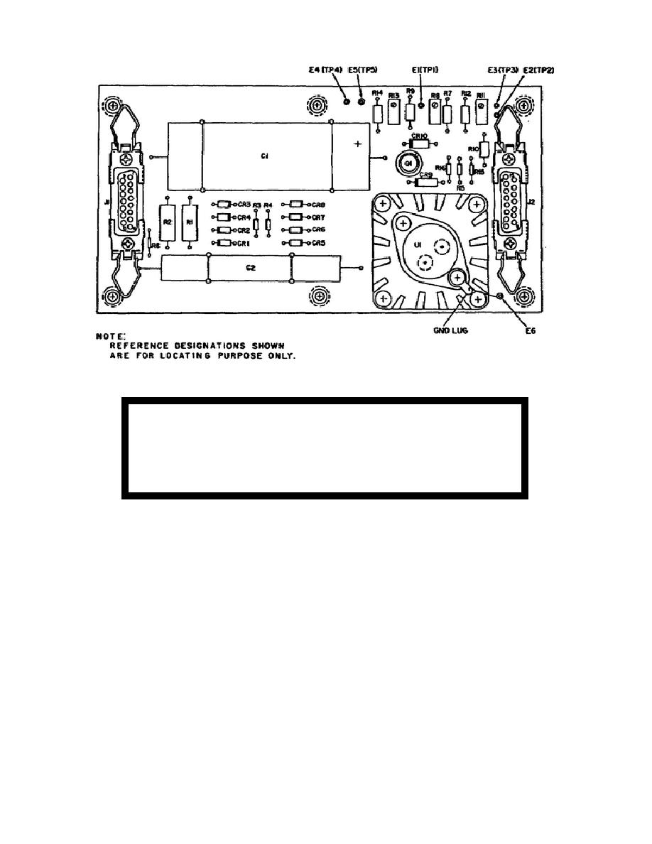
• Home
  • Download PDF
  • Order CD-ROM
  • Order in Print

Home > Ordnance Documents and other related manuals > > Figure 1-18 Power Supply Board Layout Diagram.
Figure 1-15. Special Tools And Test Equipment.
Figure1-19 Electronics Board Layout Diagram

Troubleshooting ther AN/ GVS-5 Laser Observation Devise Test Set, TS-3620
Page Navigation
  19    20    21    22    23  24  25    26    27    28    29  

Figure 1-18.
Power Supply Board Layout Diagram.
WARNING
High voltage may be present on exposed terminals.
Use care when measuring.

Set the ON/TRIPPED OFF circuit breaker (figure 1-9, item 23)
to TRIPPED OFF.

Remove the AC power cable assembly (figure 1-9, item 2) from
the PWR jack (figure 1-9, item 26).

Remove the LR Tester from the base.

Remove W1P1 from A2J1 (figure 1-11, item 10).

Remove A1P1 from A3J2 (figure 1-11, item 29).

Connect the AC power cable assembly on the power jack.
24
OD1716


Western Governors University

< Previous Page
Index ^
Next Page >

Privacy Statement
Press Release
Contact

© Copyright Integrated Publishing, Inc.. All Rights Reserved. Design by Strategico.