

ELECTRONIC PRINCIPLES - OD1647 - LESSON 1/TASK 2
mistakenly biased in the forward direction, the excessive
current could develop enough heat to destroy junctions, making
the transistor useless. Therefore, be sure bias voltage
polarities are correct before making any electrical connections.
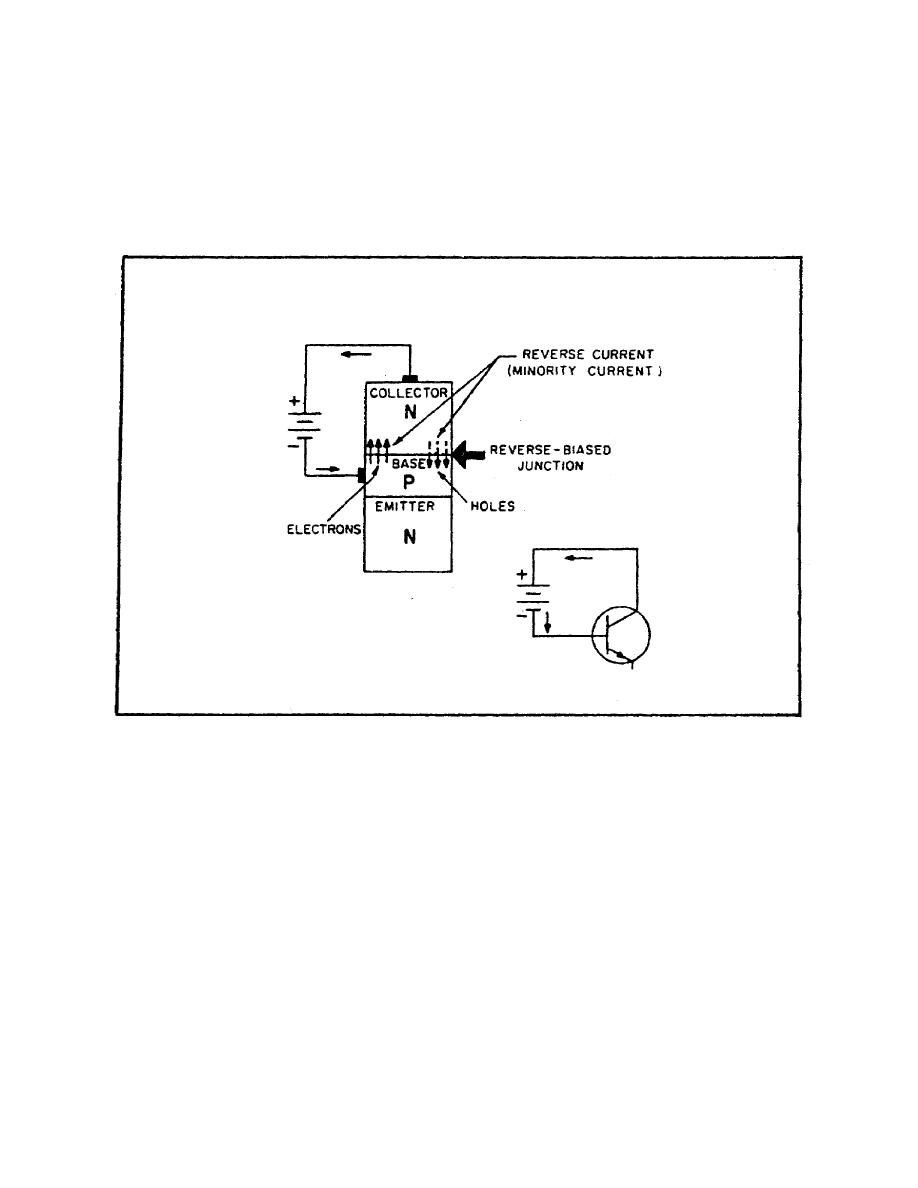
FIGURE 90. REVERSEBIASED JUNCTION IN AN NPN TRANSISTOR.
(3) NPN Interaction. For a better understanding of just how
the two junctions of the NPN transistor work together, refer to
figure 91 on the following page.
The bias batteries in this figure have been labeled Vcc for the
collector voltage supply, and VBB for the base voltage supply.
The base supply battery is quite small, as indicated by the
number of cells in the battery, usually 1 volt or less.
However, the collector supply is generally much higher than the
base supply, normally around 6 volts. This difference in supply
voltages is necessary in order to have current flow from the
emitter to the collector.
126


 Previous Page
